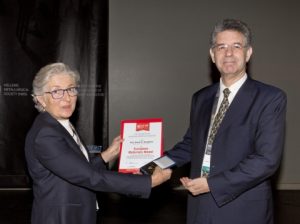
FEMS European Materials Medal 2017
Prof. Doros N. Theodorou
School of Chemical Engineering, National Technical University of Athens, Greece
“Molecular Modelling of Materials: Promises, Challenges, and Impact”
Molecular-based approaches for understanding and tailoring structure-property processing relations in materials, based on the fundamental principles of quantum and statistical mechanics, have gained ground in academic research and industrial practice. They have been greatly aided by an unprecedented growth in computer power, but also by new, efficient theoretical and computational methods and algorithms. The broad spectra of length and time scales governing structure and dynamics in real-life materials have demanded the advancement of multiscale modelling strategies, involving more than one levels of representation, to bridge atomistic constitution and interactions with macroscopic properties. In this talk we will discuss examples of molecular modelling of polymeric and nanostructured materials, addressing questions such as: How can we push the frontiers of predictability by appropriate design of multiscale theoretical and simulation approaches? Can computational high-throughput screening guide experimental efforts towards the development of new materials? What is the impact of materials modelling in industrial environments?
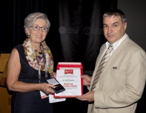
Materials Innovation Medal 2017
Dr. Thierry Chartier
Science des Procedes Ceramiques et de Traitements de Surface (SPCTS European Ceramic Center, France
Additive Manufacturing of ceramics: a new way to design and fabricate advanced ceramic parts
Since their introduction in the late 1980s, additive manufacturing technologies (AM) have become very attractive to produce accurate parts via an automated process. The part is directly built up from a computer-aided-design (CAD) file, allowing the user to have an immediate response on the shape, function or performance of the object.
Used in a wide range of industries, AM allows companies to turn innovative ideas into successful end products rapidly and efficiently. Depending on the nature of the final object, the AM techniques can be used to produce a cost-effective single item or a low – volume manufacturing. Today, AM technologies are currently becoming real manufacturing processes in various industrial fields. In the domain of ceramics, AM technologies constitute an attractive answer to the need of shaping techniques to produce useful complex parts and specific architectures which cannot be produced with a traditional method, without costly tooling and/or machining. AM technologies of ceramics are flexible techniques that offer the ability to directly redesign parts (shape/dimensions) in the CAD file to optimize a property, restricted by conventional manufacturing methods, and with the great advantage not to have to modify the tooling. Additive processes are likely going to transform the field of ceramic manufacturing and will open new ways of thinking about objects design and fabrication of advanced ceramic with improved or new functions. AM technologies used in the ceramic domain, such as, Binder jetting, Robocasting, Ink-jet printing, Selective laser sintering and Stereo lithography, are used or under development to build 3D ceramic parts. Among these methods, the space-resolved UV photo polymerization of a reactive ceramic system (Stereo lithography) presents the advantage to makes it possible to fabricate useful, dense complex 3D objects, with a high dimensional resolution, a good surface finish and properties similar to those obtained by classical routes. This process is used to design and fabricate innovative advanced ceramic components for various applications (space, telecommunication, biomedical, engineering, jewellery…) requiring specific properties.
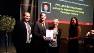
Prof. Andres-Fabian Lasagni
Institute for Manufacturing Technology TU Dresden, Germany Fraunhofer-Institut fur Werkstoff-und Strahltechnik IWS,Dresden, Germany
“Bridging the gap between high resolution laser structuring and high throughput using Direct Laser Interference Patterning”
Starting from a simple concept, transferring the shape of an interference pattern directly to the surface of a material, the method of Direct Laser Interference Patterning (DLIP) has been continuously developed in the last 20 years. From lamp pumped to high power diode-pumped lasers, DLIP permits today for the achievement of impressive processing speeds, even close to 1 m²/min. The objective: to improve the performance of surfaces by the use of periodically ordered micro and nanostructures. This study describes the advances performed in the DLIP method, with the objective of bringing this technology to real industrial applications. From the structuring of thin metallic films to bulk materials using nano – and picosecond laser systems, going through different optical setups and industrial systems which have been recently developed. Several technological applications are discussed. In all cases, DLIP has not only shown to provide outstanding surface properties but also outstanding economic advantages compared to traditional methods.
Posted by Federation of European Materials Societies (FEMS)
